



Global Chipmakers Plan High-NA EUV Production
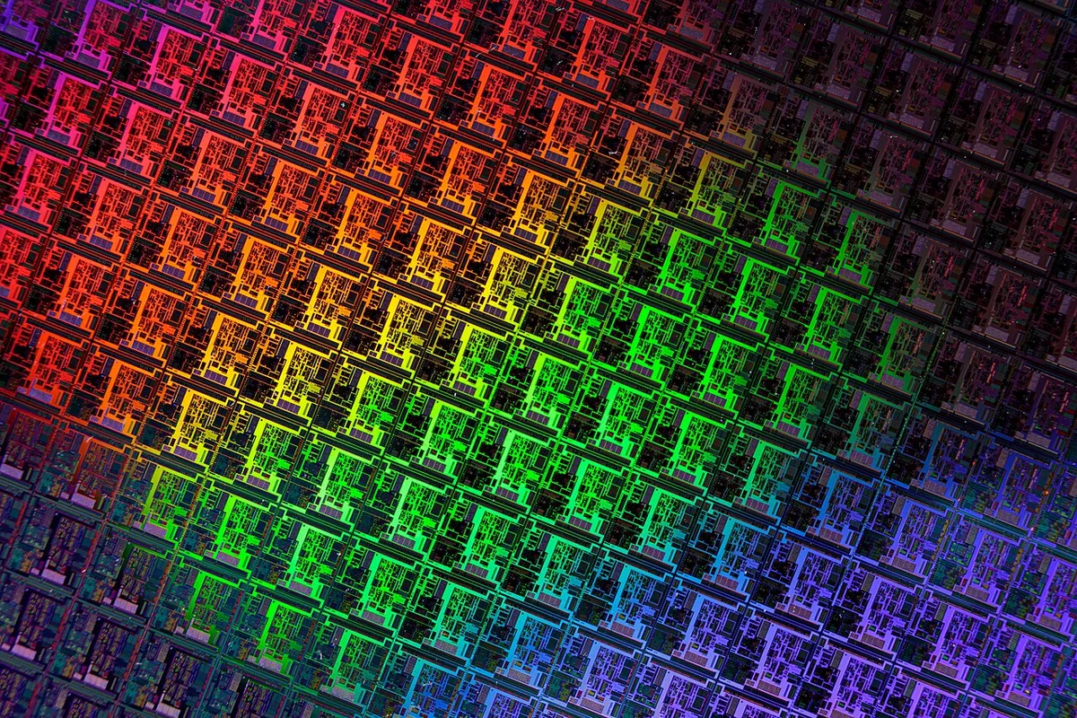
Samsung plans to introduce ASML’s High-NA extreme ultraviolet lithography in DRAM mass production by 2028, potentially enabling finer patterns, fewer manufacturing steps and greater fabrication efficiency. SK Hynix is pursuing a similar 2028 timeline, while TSMC is targeting around 2030 and Intel has already begun using the technology in high-volume production. Because High-NA systems have smaller exposure fields, Samsung, Intel and other industry participants are supporting a shift from six-inch to 12-inch photomasks, which could reduce stitching requirements and improve productivity. The machines cost roughly $400 million each, and strong advance demand is giving ASML clearer revenue visibility while placing higher equipment costs on chipmakers. The technology is being positioned as an important enabler for advanced memory, AI processors and sub-3-nanometer manufacturing, although adoption will depend on equipment capacity, process integration and yield improvements.